Archive for 2014

New blog

Friday, November 7th, 2014

Have finally got around to moving to an updated backend/infra database. Will be posting all my subsequent blog posts from here. Have titled this as Travelling on the Silicon Road - Part 2. I plan to write more on management and strategy issues with specific insights to the semiconductor world in this blog.

Are you capturing enough value on your innovation?

Monday, November 3rd, 2014

Read an interesting article, “Capture more value” by Stefan Michel in the latest HBR issue (October 2014). The article talks about how companies while putting in efforts in value creation often lose focus on value capture, thus leaving money on the table. It describes 5 different innovation categories in value capture – Changing the price setting mechanism, changing the payer, changing the price carrier, and lastly changing the segment.

Value Capture

Most of us in the semiconductor industry would confess to be “techno snobbish “. Working at leading edge technologies and in the scaling race, we often miss out the salient point – customers want technology benefits and not technology per se. While we are steadily moving towards treating the hardware chips and systems as modes for creating value and not just solely numbers in nanometres, we have a long way to go in exploring various possible and often innovative ways on how we can optimally leverage the value we create. Value capture is sadly under prioritized.

Let me take a few examples on some varying stages of value capture in this industry…..

Capturing value by changing the price setting mechanism:
The idea is to set the price according to the product’s value or worth to the customer. Memory (DRAM and NAND Flash) pricing is a good example here.

Changing the price carrier:
Price carrier is what the seller is hanging the price tag on. Semiconductor IPs is a good example here. IP vendors have evolved their IP strategies from treating IPs as fillers for differentiating hardware sockets in a system towards ensuring that the IP works not just as an isolated unit but also in the complete system. It subsequently evolved towards IP plus services and then is moving towards offering the customer a complete IP (hardware, services, software) platform solution. The price tag has moved from the die space to differentiating value provided to the customer and then the complete valued package. Bundling and unbundling of various EDA licenses is another example where the EDA company is changing the price carrier.

Changing the payer:
It may not always be the case that it is only the consumer of the product/offering who pays for the value he receives. Like in some media where content is offered free to the public, the costs are shared by the advertisers. An example I see here is that of Qualcomm’s push to the China fabless design houses to design using its cores. Am not sure of the veracity of this but understand that in China, Qualcomm recovers its IP royalty not from the design houses there but from the system houses which use the design solution (with the Qualcomm core) from these local design houses.

One of the potential big biz for us is in the Internet of Things….. and it is especially in this space that the semiconductor industry needs to think hard and differently from its traditional value innovation and capture strategy - if it doesn’t want to be left out with just a fraction of the pie. I will do a separate post on this shortly.

Do you see other examples of value capture in your industry? What is your opinion on this? Would be keen to hear your ideas and perspective on this.

R&D Efficiency

Thursday, August 28th, 2014

Anticipating customer requirements – often implicit – and identifying technology trends early in the product or technology development cycle in order to have a sustained revenue growth is crucial for any high technology industry. It is more so in the semiconductor industry which has its own economic cycles (typically 4 years of crests and troughs), high costs and technological complexities. Throw in the uncertain macroeconomic conditions coupled with increasingly dynamic and uncertainty in gauging market needs, shortening market window availability and the spiralling costs of trying to stay on the leading edge. And what does one have – a highly challenged R&D team with limited resources and the pressure to stay perched, if not ahead, on the curve.
And this is where R&D Efficiency gets all the more critical.
R&D Efficiency is the Return on the R&D investment, a tangible measure of what an entity gets for the number of R&D dollars invested.

Traditionally, the R&D team’s objectives are set along with inputs from the Biz and Technology Strategy group, Marketing & Sales group and sometimes the Field Application groups (usually a highly under leveraged asset) – and being aligned with the company’s top level vision and objective and with the available resources. Once handed down with the R&D mandate, the various R&D teams get onto what they have been trained to do best – R&D. And these mostly get done in silos with not much of active bridges of communication, let alone brain storming, between each other.

In my last post, Mining the seams, I mentioned about facilitating R&D folks to be market savvy – not to turn them into marketers but to facilitate in aligning R&D investments with market needs and achieve R&D efficiency. Having recognized that an issue exists is the first step. Making the necessary steps for the transformation follows. And this is especially catalyzed when all indicators point that maintaining the status-quo will be more dangerous than venturing into unknown.

Quite often even the well intentioned initiatives get watered down during the implementation or transformation phase. A new design flow, a more efficient way of mapping the customer requirements into your product/technology roadmap, moving into adjacencies, hedging R&D bets etc. are often “lost in translation”.

I revisited an old HBR article recently which throws light on how one can lead a sustainable transformation in an organization. It is titled, “Leading Change: why transformation fails” by John P. Kotter.
It lists 8 steps in transforming your organization:
• Establishing a sense of urgency
• Forming a powerful guiding coalition
• Creating a vision
• Communicating a vision
• Empowering others to act on the vision
• Planning for and creating short-term wins
• Consolidating improvements and producing still more change
• Institutionalizing new approaches

It is a very interesting and informative piece and would serve us well to keep in mind while transforming to increase our entity’s R&D efficiency.

Mining the seams

Friday, August 22nd, 2014

This was the phrase that actually caught my attention in an informative article, “Decision making Marketing” in the HBR July-Aug ‘14 issue.

The main problem in decision making referred to in the article is the communication falling through across the different silos in an organization thus impeding effective decision making. Challenges include divergent assumptions, lack of alignment and shared commitment across the organization structures - amongst others. Reorganizing the structure/reporting doesn’t often address this completely. Sometimes it just creates more or different silos and the challenge remains unaddressed. Mining the seams helps address this by working closely across functions, avoiding organization bottlenecks and getting work done quicker and more efficiently than in the past. While the article mainly talks about the challenges involved in decision making for marketers when they need to communicate across domains of product development, sales, finance etc., the same is true for any other function too.

Here are my thoughts mapping this to the various spaces I worked in …Am keeping mining the seams as central (rather than decision making) and I may be taking another interpretation and possibly an extension of the main theme from the article.

An IC development program requires close interaction between various functions – Marketing, Design, Manufacture, Planning, Packaging, Testing, IP, Finance, Legal etc. Islands of expertise in each can be found aplenty. However what are rare and very much needed are people who can effectively communicate across these seams for decisions made in various phases of the chip development affect others. A design decision taken in isolation from say packaging can result in a major chip gaffe.

Another example is the R&D functions in an organization. Going by Donald Stoke’s model, one can lean towards pure research (Bohr) or gravitate more towards the applications part (Edison) or find a central niche (Pasteur). For those in the latter two especially, we see a major need to mine the seams. R&D professionals need to align their research to the market requirements and move towards what can be termed – Technology substitution to Technology Epiphany. These means getting out of their labs and well……..mine the seams. Aligning market research to your innovation requirements, mapping the customer needs (explicit or implicit, existing or potential) to your R&D or technology road map needs effective communication across functions…mine the seams.

I regularly conduct training workshops for facilitating R&D folks to be market savvy – not to turn them into marketers but to facilitate in aligning R&D investments with market needs and achieve R&D efficiency. Absence of communication to communication falling through the seams is issues frequently observed.

The first step is to recognize the issue exists – it is surprising how many of us are in a state of denial. Strategies and tools are available to address the challenge.

One of the initiatives taken is to have cross functional teams to facilitate the communication flow. However in most places, these work on “passing the baton” theme rather than “playing the new new product development game” a concept proposed by Hirotaka Takeuchi and Ikurjiro Nonaka – “Stop running the relay race and take up rugby” – the ball gets passed back and forth within the team as it moves as a unit up the field.
Temporary teams set up for a project and disbanded on project completion is another way. The teams here owe their commitment to the project rather than solely to the departments they belong to. Requires tweaking the KPI and other performance markers but such dynamic structures have shown good results.

It pays to mine the seams!

Semiconductor and Cloud

Wednesday, June 4th, 2014

A couple of years back, I had given a talk as well as moderated a panel on chip design and cloud. I had written about the same later in one of my blog posts, Chip designing and the Cloud.

I ended the article with “In summary, cloud computing in chip design will be a big paradigm shift and is poised to bring about tremendous benefits to the design eco-system. However for the design community to actively adopt it, the relevant stakeholders need to look into it in a holistic way and much beyond the scalable and economic computing power and data storage combo. And this may very well redefine the existing chip design methodology.”

So the recent news on Silicon Cloud International bringing together ecosystem partners for chip design at DAC was quite heartening to note.

SCI establishes secure cloud computing centers for scientific and engineering applications across the world. As an initial application, SCI’s cloud is providing turn-key design-to-manufacturing semiconductor design workflows for universities and research institutions. SCI’s private cloud and thin client architecture establishes a novel security model for semiconductor ecosystem providers and users.

IEDM 2014 call for papers - submission deadline 23rd June

Friday, May 30th, 2014

IEDM
A call out to the best scientists and engineers in the field of microelectronics from industry, academia and government ….

The 60th annual IEEE International Electron Devices Meeting (IEDM) has issued a Call for Papers seeking the world’s best original work in all areas of microelectronics research and development.

Papers in the following areas are encouraged:
. Circuit and Device Interaction
. Characterization, Reliability and Yield
. Display and Imaging Systems
. Memory Technology
. Modeling and Simulation
. Nano Device Technology
. Power and Compound Semiconductor Devices
. Process and Manufacturing Technology
. Sensors, MEMS and BioMEMS

The 2014 IEDM will take place at the Hilton San Francisco Union Square Hotel from December 15-17, 2014.
So if you qualify yourself in the above league, well, rush off your submissions as the deadline for the papers is June 23. Good luck!

Details at IEDM 2014 home page at www.ieee-iedm.org

Mobility and IoT - and its impact on the semiconductor industry

Monday, April 28th, 2014

I attended the Semicon 2014 last week here in Singapore at the Marina Bay Sands – after a self-imposed hiatus of a few years. I attribute the hiatus to Semi charging people to attend its industry tracks. I do realize that they too have to make a bit of money to sustain but then it is always tough to pay for an event once you get used to participating in them for free for some years! Anyhow, as I was chairing a session on the Fabless/IDM Technology Challenges track in this year’s event, I had free access to all its tracks and especially the market trends as well as the networking cocktail event held on the first day. The market trend has always been a big crowd puller for Semi and this year was no exception.

img1

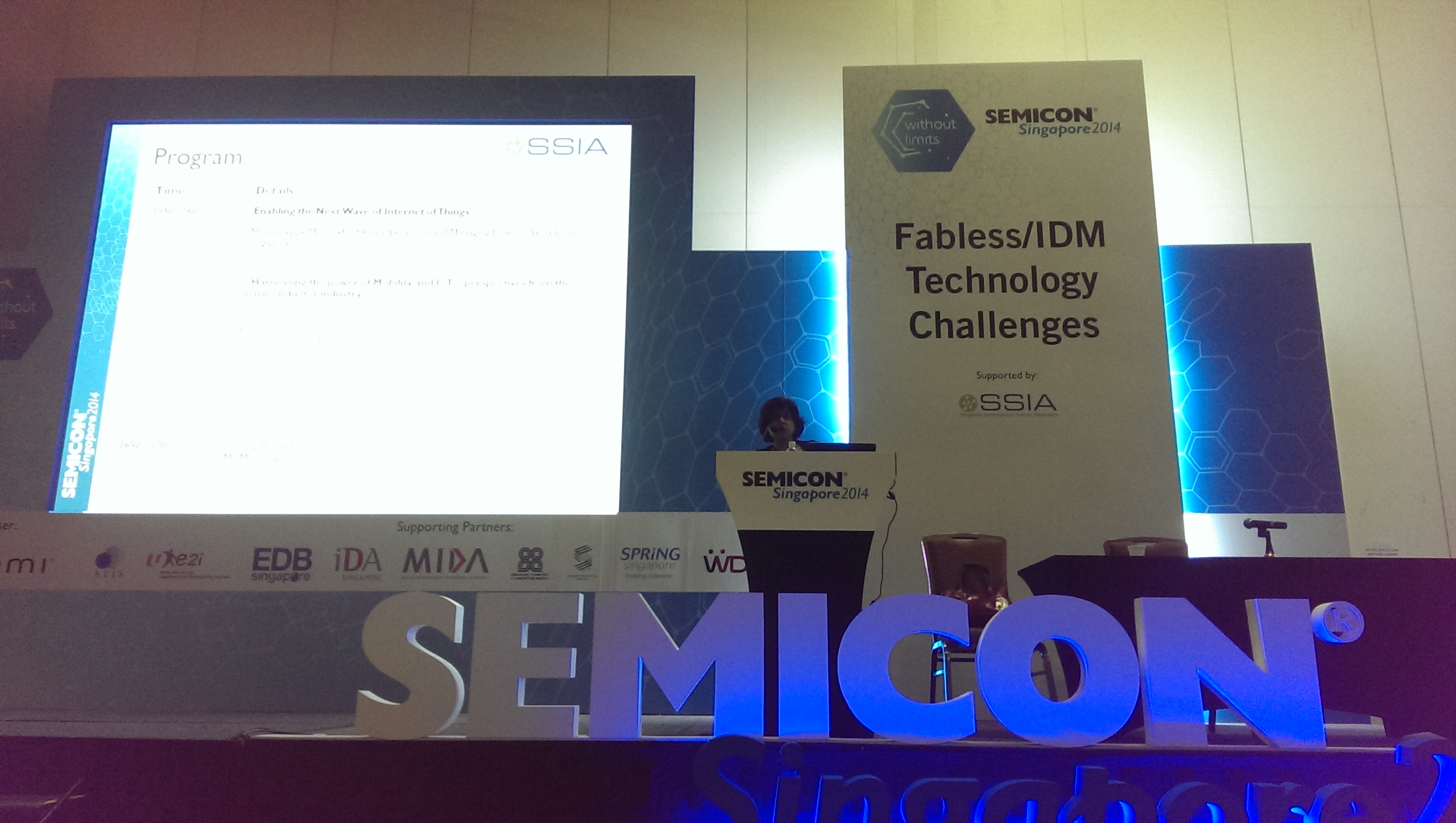
Anyhow, let me talk here about the Fabless/IDM track. This was co-organized by SSIA (Singapore Semiconductor Industry Association) of which I happen to be an executive committee member, along with Semi.

The theme of this track was “Mobility and IoT - and its impact on the semiconductor industry “. The growth has been quite rapid in this space especially now in the IoT one. The potential market is huge, is fragmented and with low barriers to entry and no major competitors/players (as yet) – a conducive backdrop on Porter’s five competitive forces shaping industry competition. Unlike the smartphone market which has evolved into a cut throat biz dominated by vertically integrated players, the IoT looks set to provide a refreshing levelling impetus.

We are looking into some exciting and innovating market opportunities in this space, especially on the IoT front. Apart from the potentially high growth applications markets that this opens up for the semiconductor industry, the underlying fabric of our industry is also seeing transformation at various levels including the increasing inter dependency and synergy across the various entities in this eco system. These emerging application markets and morphing industry ecosystem bring along several interesting visions and opportunities as well as new challenges. So it was with a lot of excitement and quest for knowing more on this aspect that I was looking forward to chairing this session and especially more to moderating the panel discussion following the presentations. And of course, the great speakers and the panellist line-up fuelled this up.

The speakers included Vincent Tong, SVP, New Product Introductions and Worldwide Quality & Asia Pacific Executive Leader, Xilinx, Greg Turetzky, Strategic Business Development Manager, Wireless Communication Systems Group, Intel, Jennifer Teo, VP of Manufacturing and GM, Silicon Labs International and Giuseppe Miano, VP Asia Operations and MD, Broadcom, Singapore. Vincent’s talk dwelled on IoT requiring advanced SoC with differentiation as a key i.e. differentiation with intelligence and flexibility and hence programmability. Greg spoke about ubiquitous location for all mobile platforms, the opportunities and the challenges. The market opportunities have expanded from GPS to GNSS and now to location with the latter being the next big opportunity – always located and with context. Jennifer talked about how IoT is being a game changer and dwelt on the technologies required for the “things”. Giuseppe spoke about the 3rd wave of wireless connectivity – from connecting to consumption to sensing (and controlling). Have added another acronym to my vocab – BYOW (Bring your own wearable) – and must say I find that cool! He also spoke about the favourable market dynamics driving the growth as well as the aspects that need to start being considered especially on the manufacturing, logistics and suppliers side.

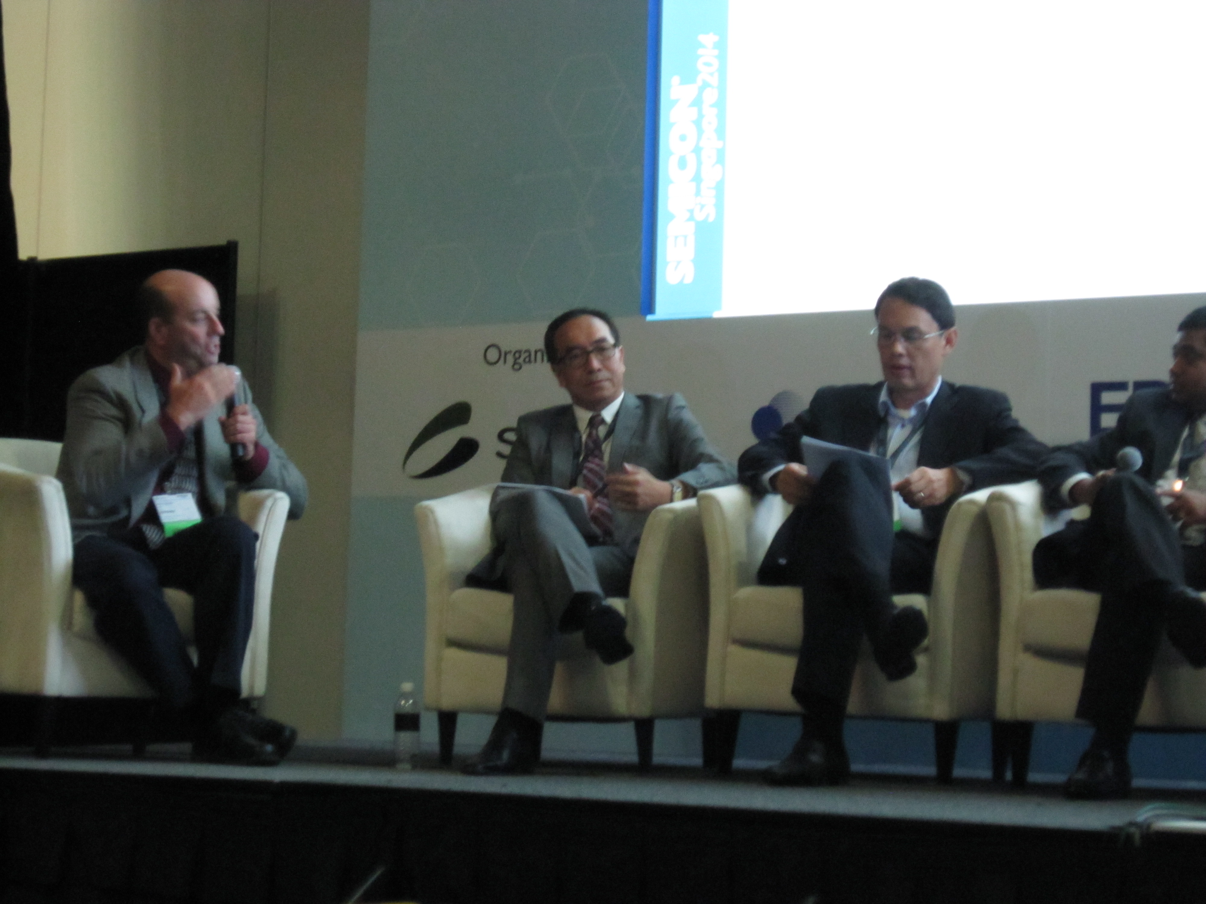
The panel discussion following these talks centred on “Harnessing the power of Mobility and IoT – perspectives from the semiconductor industry”. The panellists included the earlier speakers and
Subramani Kengeri, VP, Advanced Technology Architecture, GlobalFoundries and Francis Puno, Chairman SEA Work Group of Continua Health Alliance.

pic2

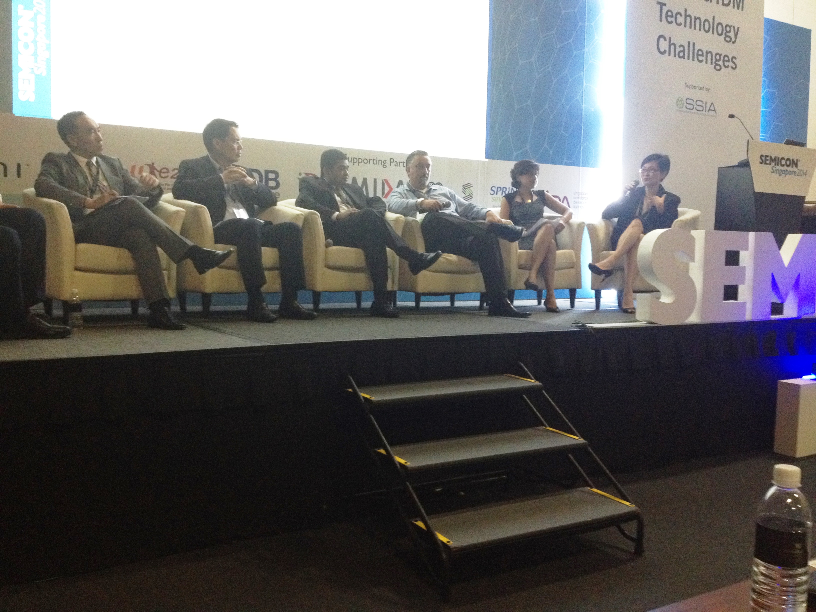
With stake holders from across the value-chain – IDM, fabless, foundry, application – the panel stirred up a lively and insightful debate. While the insights were quite forthcoming on my questions regarding the technical and even the ecosystem enablers, there was almost a conspiratorial silence from the panel on my query about the biz models they anticipated to develop or emerge with IoT applications. As they said, everyone is holding their cards close to their chest!

It was an insightful and a highly engaging session where all the speakers and panelists spoke passionately about this industry. And that is always heartening!

pic3

Fabless & IDM Technology Challenges track in Semicon Singapore 2014

Monday, March 17th, 2014

Join me in this track that Singapore Semiconductor Industry Association (SSIA) is organizing along with Semi in the Semicon Singapore 2014 on 23rd April 2014 (1330 – 1700 hours) at TECH West, Marina Bay Sands.

The theme of this track is “Mobility and IoT - and its impact on the semiconductor industry “

Mobility, especially in the consumer devices was one of the major revenue drivers in 2013. Joining it now, we are seeing a resurgent growth of Internet of Things (IoT) and wearable devices. We are looking into some exciting and innovating market opportunities in this space. Apart from the potentially high growth applications markets that this opens up for the semiconductor industry, the underlying fabric of our industry is also seeing transformation at various levels including the increasing inter dependency and synergy across the various entities in this eco system.

These emerging application markets and morphing industry ecosystem bring along several interesting visions and opportunities as well as new challenges. Hear from some of the industry leaders including ones from Broadcom, Intel, Silicon Laboratories and Xilinx on the emerging industry dynamics that are paving way for new biz and growth opportunities in the Mobility and IoT space as well as the associated challenges - and with additional emphasis on what and how these perspectives relate to the Singapore semiconductor landscape.

Speakers and their talks include
• Ubiquitous Location: Challenges and opportunities of enabling all-day, everywhere location for all mobile platforms - Mr Greg Turetzky, Strategic Business Development Manager, Wireless Communication Systems Group, Intel


• How the Internet of Things will change our world - Ms Jennifer Teong, Vice President of Manufacturing and General Manager, Silicon Labs International


• Enabling the next wave of Internet of Things - Mr Giuseppe Miano, Vice President of Asia Operations and - Managing Director, Broadcom, Singapore


• Mr Vincent Tong, Senior Vice President, New Product Introductions and Worldwide Quality & Asia Pacific Executive Leader, Xilinx

The talks will be followed by a panel discussion, “Harnessing the power of Mobility and IoT – perspectives from the semiconductor industry” which will strive to shed some light on these two game changers – Mobility and IoT – from the eyes and ears of the semiconductor industry.

Panellists include


• Above speakers and

• Mr Subramani Kengeri, Vice President, Advanced Technology Architecture, GlobalFoundries

• Mr Francis Puno, Head of Business Development –mHealth, Spice Global
Panel
• Moderator: Ms Meenu Sarin, Director, VLSI Consultancy, Assistant Honorary Secretary - Singapore Semiconductor Industry Association (SSIA)

You may access the Program and registration details at www.ssia.org.sg


I look forward to seeing you at this track!